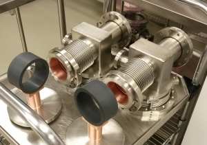
NCBJ will assist Kubara Lamina S.A. to deliver parts ordered for an US research super-laser
14-09-2017
NCBJ / Kubara Lamina S.A. joint press release
NCBJ and the Kubara Lamina S.A. company have reached framework agreement on cooperation, according to which NCBJ will conduct research, make test measurements, and technically evaluate microwave equipment produced by the partner, including parts ordered for the LCLS free electron laser currently under development at Stanford University in California. The order has come after successful accomplishment of an order for similar equipment for the European XFEL laser in Hamburg delivered jointly by NCBJ and Kubara Lamina.
Profile of Kubara Lamina S.A., a company located in Piaseczno near Warsaw, includes microwave devices/subassemblies for aviation and military applications. In cooperation with numerous research institutions the company has also been producing some unique microwave elements. In 2017 the DoE agency of the US government selected the company as supplier of some microwave subassemblies for the Linac Coherent Light Source (LCLS-II) free electron laser currently under development at the SLAC lab (Stanford University, California).
NCBJ has already cooperated with Kubara Lamina to manufacture some microwave subassemblies for the European XFEL X-ray Free Electron Laser recently put in operation in Hamburg (Germany). „It was a very fruitful relationship, satisfying both partners, I hope” – said D.Sc. Krzysztof Kurek, NCBJ Director General. „Scientists and designers, but also industrial partners accomplishing projects to develop large research facilities such as XFEL must inevitably face some yet unexplored challenges. At every step something not yet done before must be done. Successful accomplishment of such a project always brings plenty of satisfaction and such record is a strong asset in any competition for further orders”.
„Our tasks in the XFEL project included to manufacture over one hundred absorbers of higher modes of electromagnetic field. Their function was to absorb unwanted frequencies capable to interfere with accelerating of particles within the accelerator” – explained Wojciech Grabowski, MSc from NCBJ Division of Physics and Technology of Particle Acceleration. „At a glance absorbers are just tee-like constructions made of steel pipes. However, some details placed inside the construction are not trivial. Some absorber elements must be electroplated with nickel and copper. Such electroplating is quite a difficult technological operation and we searched for a subcontractor who would take on the task all over Europe. The basic problem is that nickel is a ferromagnetic metal, while it would be unacceptable if the coating magnetically disturbed the electroplated structure. The problem was further compounded by the very complicated shape of the to-be-electroplated internal surfaces. Kubara Lamina accepted the order and they did some excellent work”.
„Experience gained during fulfilling the order for XFEL elements enabled us to win a contract for deliveries of similar details for the laser currently under construction in SLAC” – said Jerzy Kubara, President of Kubara Lamina S.A. – „We are very proud that in the competition we have defeated some recognized US companies. It is not our first contract won in the USA. We have been delivering some high power supply subassemblies to US railroad industry and military aviation for many years”.
NCBJ / Kubara Lamina agreement is a framework one. „ Within framework of that agreement we would like numerous materials and workpieces produced by us to be tested for their magnetic, electric and absorption properties” – said Mariusz Błażejewicz, R&D Director in Kubara Lamina S.A. – „We hope NCBJ will help us to determine chemical composition of some of the materials used by us to manufacture absorber components. We also hope for technical consulting on the technology of cleaning and testing some absorber elements. We plan to test in NCBJ labs quality of each of our products to be sent to Stanford”.
About KUBARA LAMINA S.A. in Piaseczno:
Formerly Zakłady Elektronowe LAMINA S.A., KUBARA LAMINA S.A. has been a major manufacturer of microwave and high power semiconductor products in Poland for 60 years. Technological operations applied in manufacture of semiconductor devices include photolithography, diffusion, soldering, chemical treatment, evaporation of aluminium/gold contacts, device assembly. Operations applied in manufacture of vacuum products include machining, electroplating, high vacuum pumping, metal/ceramics or metal/glass brazing. All products are manufactured to top quality standards and meet the EN ISO 9001:2008, PN-EN ISO 9001:2009, and AQAP 2110:2009 industry standards. See company Webpage at www.kubaralamina.com.
