English
 Polish
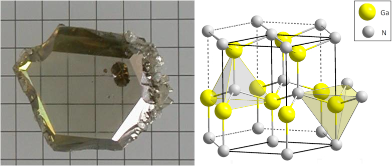
NCBJ researchers are testing the radiation resistance of materials for high-power electronics
16-07-2026
Electronics based on gallium nitride (GaN) can be significantly more resistant to radiation-induced defects than silicon-based solutions. This makes it a good candidate for use in extreme conditions, such as in nuclear reactors or space missions. To better understand the behaviour of gallium nitride under the influence of radiation, a team of scientists from the National Centre for Nuclear Research, the Institute of High Pressure Physics of the Polish Academy of Sciences and the University of Lisbon investigated the mechanisms of defect formation depending on the fabrication method and the polarity of GaN crystals.
Silicon is the foundation of modern electronics. This element is widely found on Earth, and methods for producing its monocrystals were developed as early as the beginning of the 20th century (such as the Czochralski method). However, the development of electronics in recent years has led physicists and engineers to seek out other semiconductor materials whose properties are better suited to the conditions in which they will operate. One such group turned out to be III-nitrides, particularly gallium nitride (GaN). As a semiconductor, it can compete with silicon, and its unique properties mean it performs exceptionally well in high-power and high-frequency electronics, including microwave device components, radiation sensors and LEDs.
A key property of GaN is its high resistance to the formation of defects under the influence of ionising radiation. This allows the material to be used in extremely harsh conditions, such as modern nuclear reactors, accelerators or space missions. However, to ensure the reliable operation of such components, the behaviour of GaN under irradiation must be thoroughly understood. Scientists have focused particular attention on the differences in this material’s response to irradiation, depending on the method used to produce the gallium nitride crystals. Furthermore, recent studies have shown that the orientation of GaN crystals has a significant impact on the performance of the resulting components, which introduces an additional variable in the analyses.
A group of scientists led by dr Przemysław Jóźwik from the Synthesis and Characterisation of Materials Division at the National Centre for Nuclear Research undertook a detailed study of the formation and accumulation of defects in gallium nitride bombarded with argon ions. The analyses were carried out in collaboration with specialists from the Institute of High Pressures of the Polish Academy of Sciences and the Institute of Plasma and Nuclear Fusion at the University of Lisbon. The results have just been published in the prestigious journal New Journal of Physics.
In their work, the researchers took into account both the method of material production and the polarity (orientation) of the crystals. The analyses combined experimental methods (Rutherford backscattering spectrometry in channeling mode, RBS/C) and computer modelling using the McChasy software developed at the NCBJ.
– The research shows that the structure and method of GaN production strongly influence the type and rate of defect formation: from point defects to dislocation loops. In the case of materials with different polarities, we also observe distinct differences in the level of damage, particularly for crystals produced using the HVPE epitaxial method – explains dr Przemysław Jóźwik of the NCBJ, the first author of the paper.
Research shows that GaN produced by the ammonothermal method (crystallisation from an ammonia solution at high temperature and pressure) has a dislocation density up to 100 times lower, but is significantly more prone to defect formation. Analyses of different argon beam doses also indicate that, regardless of the fabrication method, a transformation of defects occurs at a certain fluence.
Further work will enable a precise determination of the effect of radiation intensity on defect accumulation. In addition, the authors plan to investigate the behaviour of defects during the annealing of components. This research will provide a better understanding of the mechanisms affecting gallium nitride-based electronics, reducing the risk of damage to electronics that must operate under extreme conditions.
The research results are available in the publication: Przemysław Jóźwik et al,. Polarity and fabrication effects in Ar‐bombarded GaN, 2026, New J. Phys. 28 073501, DOI: https://doi.org/10.1088/1367-2630/ae8570